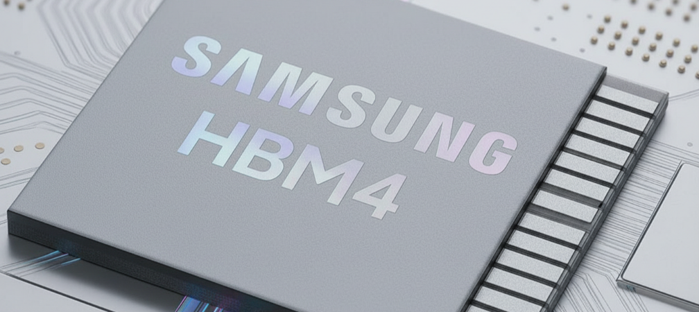
Samsung to more than double HBM4 and HBM4E output
TL;DR: Samsung is expected to more than double output of its HBM4 and HBM4E high-bandwidth memory next year, and the first hard evidence is not a press release but a procurement number: outsourced cleaning of the glass carriers used in HBM production is set to rise to 50,000 sheets a month from 20,000. Total HBM wafer starts are projected to climb about 40% to roughly 250,000 a month, with the HBM4 family going from around 40% of shipments to about 80%. More HBM4 capacity means more memory going to AI accelerators rather than to ordinary laptops — which is exactly why the RAM you buy in Malaysia is still getting more expensive.
Samsung Electronics has spent most of 2026 telling the market that its sixth-generation high-bandwidth memory is back on track. The newest supply-chain numbers say the same thing, only louder, and they say it in a way that is hard to dress up: the company is ordering consumables at volumes that only make sense if HBM4 and HBM4E output is about to roughly double.
The estimate does not come from Samsung guidance. It comes from the temporary glass supports that hold a wafer flat while it is ground down to a fraction of its original thickness — an unglamorous input whose purchase volume is one of the few visible proxies for how much stacked DRAM a company intends to build.
What Samsung’s glass-carrier order really signals about HBM4 output
Samsung will raise outsourced cleaning volume for glass carriers to 50,000 sheets a month next year, up from 20,000 sheets a month this year, according to industry sources cited by Seoul Economic Daily on 20 September 2026. As recently as last year, the company needed only 10,000 sheets a month.
That trajectory matters because glass carriers are reused. They are bonded to the underside of an HBM DRAM wafer, hold it flat through the thinning and drilling steps, and are then detached, cleaned and cycled back into the line. Because they are reused, a 2.5-fold jump in cleaning volume is a demand signal rather than a one-off purchase.
Industry officials quoted in the same report say the figure points to HBM4 and HBM4E output at least doubling from this year — even after allowing for reuse cycles and for the way consumption varies with process loading and yield. Cleaning is a service that scales with how many carrier cycles a fab runs; carrier cycles scale with how many wafers get thinned; and wafers get thinned because they are destined for stacked HBM.
The same sourcing describes a wider HBM expansion: total HBM production measured by average monthly wafer starts is expected to grow nearly 40%, from roughly 180,000 wafers a month this year to about 250,000 next year. Within that total, the mix shifts decisively upward. The HBM4 family — sixth-generation HBM4 and seventh-generation HBM4E — is projected to move from around 40% of shipments this year to approximately 80% next year as HBM4E mass production gets fully under way.
One industry official quoted in the report put the commercial logic plainly: as Samsung expands HBM output, it appears to be placing HBM4, a high-value product, at the centre.
Two caveats are worth holding onto. The figures come from unnamed semiconductor industry sources and unnamed analysts, not from a Samsung disclosure, and the doubling is a projection that already bakes in carrier reuse and yield variability rather than a guaranteed outcome. Samsung has so far declined to confirm wafer-level or carrier-level numbers.
The numbers behind the HBM4 output doubling
Stripped of the sourcing detail, the picture looks like this:
| Metric | This year (2026) | Next year (2027) |
|---|---|---|
| Glass-carrier cleaning volume | 20,000 sheets/month | 50,000 sheets/month (+150%) |
| Glass-carrier requirement, prior year | 10,000 sheets/month (2025) | — |
| Total HBM wafer starts | ~180,000 wafers/month | ~250,000 wafers/month (+~40%) |
| HBM4-family share of HBM shipments | ~40% | ~80% |
| Implied HBM4 / HBM4E output | baseline | at least 2x |
Read the top and bottom rows together and the strategy is obvious. A 2.5x increase in a consumable used at the thinning stage, on a 40% increase in total wafer starts, means the wafers that are being added and converted are disproportionately the ones that need aggressive thinning — that is, the high-stack HBM4 and HBM4E parts, not the older, thinner-configuration products.
The mix shift from 40% to about 80% is the more important number for anyone watching memory economics. HBM4 carries a higher margin than the HBM3E it displaces, and Samsung has been reallocating capacity toward it since mid-year: by late June, roughly 75,000 of its 150,000 monthly HBM DRAM wafers were assigned to HBM4, with 8-layer HBM3E production halted and its resources redirected. That is a company deciding that the older, cheaper product is no longer worth the wafer.
Why glass carriers matter more as HBM stacks get taller
HBM is not one chip. It is a stack of DRAM dies placed side by side with a logic base die, and the whole package has to fit inside a fixed height that has barely changed across generations. Every time the industry adds layers — 8, then 12, now 12 and beyond for HBM4E — each die in the stack has to be thinner than the one before it.
Thinning happens mechanically, by grinding the back side of a completed DRAM wafer until the remaining silicon is measured in tens of microns. At that point the wafer is no longer stiff enough to hold its own shape. It warps, it bows, and it cracks when handled. The fix is a temporary carrier bonded to the underside: a rigid backing plate that keeps the thinned wafer flat while it is ground, etched, drilled for through-silicon vias, and eventually bonded into a stack.
Silicon carriers work, but glass has become the preferred material because it is flat, dimensionally stable and can be released and cleaned so the carrier can be used again. The more layers a product packs into the same package height, the thinner the dies must be, the more fragile the wafer becomes, and the more carrier cycles each finished stack consumes.
That is the mechanism that makes carrier cleaning volume a leading indicator. You cannot quietly double HBM4 output without roughly proportional growth in the carrier demand that output implies — which is why analysts treat a 2.5-fold cleaning order as evidence about products that Samsung has not yet quantified publicly.
Samsung’s HBM4 timeline: from February shipments to HBM4E samples
The ramp described by the new figures is not speculative in its early stages. It is already visible on a calendar.
Samsung began mass-production shipments of HBM4 in February 2026, the first company to do so. The part pairs sixth-generation 10-nanometre-class (1c) DRAM with a base die built on a 4-nanometre logic process — a combination that matters commercially because the base die is a logic chip, and only a company with its own foundry can design and fab both halves in-house.
In May 2026, Samsung shipped 12-layer HBM4E samples to customers including Nvidia. Sampling is the last stage before qualification, and for a memory supplier it is effectively a supply agreement in waiting: the customer tests the part, negotiates allocation, and then volume follows.
Between those two milestones, the company’s messaging turned confident. Kim Jae-jun, executive vice president of Samsung’s memory business, said on the second-quarter earnings call that HBM4 revenue in the third quarter would expand more than threefold from the previous quarter, and that in the second half HBM4 revenue would comfortably exceed 60% of total HBM revenue. Korean press reported that HBM4 had brought in about US$1 billion within four months of mass production, with annual sales projected at roughly US$10 billion.
Yield, revenue and the market-share swing behind the HBM4 ramp
A doubling plan is only credible if the manufacturing problem is solved, and on that front the news has been improving all year.
HBM4 yield sat below 60% in the early weeks of mass production in February. By August, industry sources put it close to 80% — a level reached roughly four months ahead of the internal plan, and one that clears the way for the volume commitments now showing up in carrier orders. At the same time, Samsung’s chief technology officer Song Jai-hyuk told an internal management briefing in late June that HBM4E reliability-test yield had risen above 70%, and that the company’s next-generation 1d DRAM process held an edge over competitors.
Those two numbers explain the whole strategy. Yield near 80% on HBM4 means each wafer of 1c DRAM converts into more sellable stacked memory, so adding wafers is worth more than it was six months ago. HBM4E yield above 70% at the reliability stage means the seventh generation is unlikely to slip out of next year’s window — which is what turns a 40%-to-80% shipment-mix projection from an aspiration into a plan.
The market-share picture is following. Korean reporting projects Samsung’s HBM share rising from about 27% last year to roughly 37% this year, with SK hynix easing from about 56% to 43%. TrendForce’s bit-output estimates are more conservative, putting SK hynix near 50% and Samsung up from 20% to 28%. On the specific part that matters most — HBM4 for Nvidia’s Vera Rubin platform — supply-chain analysts cited by TechTimes estimate SK hynix at roughly 60–70% of volume, Samsung at 25–30%, and Micron supplying the remainder. The direction of travel is the same in all three sets of numbers: Samsung is clawing back share in the generation where it had fallen behind.
What HBM4E adds: speed, bandwidth and efficiency
The specifications Samsung has put on the record explain why customers are willing to absorb a mix shift this fast.
HBM4 is designed to deliver consistent processing speeds of 11.7 Gbps per pin, extensible to 13 Gbps — comfortably above the 8 Gbps JEDEC baseline, and above the 10 Gbps-plus that Nvidia is reported to demand for Vera Rubin. Samsung has also shown its HCB (hybrid copper bonding) packaging technology, which it says improves thermal resistance by 20%, a meaningful figure when dozens of stacked dies run continuously next to a GPU.
HBM4E pushes further. Reporting on Samsung’s disclosures put the part at up to 16 Gbps per pin, more than 20% faster than HBM4, with aggregate bandwidth figures quoted around 3.25 TB/s across 2,048 pins, and roughly double the energy efficiency of HBM3E. The efficiency claim is arguably the most consequential, because power delivery, not peak bandwidth, is what limits how densely AI racks can be packed.
Treat vendor speed figures with the usual caution: they are targets demonstrated on reference parts, and independent verification arrives only when mass production volumes reach customers. But the direction is unambiguous — each HBM generation is buying bandwidth and efficiency rather than raw capacity, and the packaging steps that make that possible are exactly the steps that consume glass carriers.
Nvidia’s Rubin cycle and the NVHBM twist
Demand for all of this comes from a single, very specific place: Nvidia’s accelerator roadmap.
Vera Rubin entered full production after being announced at Nvidia’s GTC Taipei keynote on 1 June 2026, with Nvidia claiming 10x agent throughput at scale versus the Grace Blackwell generation. On 5 June, Jensen Huang confirmed publicly that Samsung, SK hynix and Micron had all passed certification to supply HBM4 for Vera Rubin — the first public acknowledgement that all three had cleared the bar.
Next comes Rubin Ultra, and with it a design change that plays directly to Samsung’s structure. Nvidia has introduced NVHBM, a custom high-bandwidth memory part for Rubin Ultra, reportedly requesting an 8-layer HBM4E configuration rather than the 12-layer or 16-layer stacks that have driven complexity and yield losses. Fewer layers cuts stack height by roughly a third and should lift yields, which in turn eases the memory shortage. To recover the lost capacity per stack, Nvidia is aiming at data rates around 18 Gbps, well above the 14.4 Gbps of early HBM4E samples.
Samsung’s pitch for that business rests on integration. Custom HBM requires the logic base die and the DRAM stack to be designed and manufactured as one system; Samsung can do the DRAM, the 4nm base die, the foundry work and the advanced packaging in-house, while SK hynix and Micron depend on external foundries for advanced logic base dies and packaging. If that advantage converts into an NVHBM order, production would begin next year — the same year Samsung’s carrier orders say its HBM4 family output doubles.
Who else is in the race
The doubling plan is not happening in a vacuum, and the competitive picture sets the urgency.
SK hynix remains the volume leader on the strength of its HBM3E franchise and its earlier qualification for Vera Rubin HBM4. It has been expanding capacity in parallel, starting commercial output at its new M15X fab ahead of schedule in February 2026, with initial volumes around 10,000 wafers a month and multi-fold scaling planned through the year. It also holds the larger slice of Nvidia’s HBM4 allocation today.
Micron is the third certified supplier, with a smaller share of Vera Rubin volume but a seat at the table. Beyond the big three, the industry’s constraint is starting to look structural rather than competitive: HBM cannot be fabbed out of thin air, and every wafer converted to HBM4 is a wafer not producing ordinary DDR5.
That is the context in which a 2.5x glass-carrier order becomes a story about pricing. When the most advanced memory maker triples a consumable tied to its highest-margin product, the practical effect is to pull more of the industry’s thin-wafer capacity away from commodity DRAM — and that is where Malaysian buyers feel it.
What this means for Malaysian buyers and developers
The link between HBM4 output and the price of a laptop in Klang Valley is direct, if unglamorous.
AI-focused data centres are consuming most of the industry’s new memory capacity, and every wafer dedicated to HBM is a wafer unavailable for the DDR5 and NAND that go into consumer devices. Malaysia’s tech association Pikom has called the result a “RAM crunch”. Retailers quoted by The Star described a 16GB DDR4 laptop module at a minimum of RM800, against roughly RM200 to RM400 a year earlier, and a 32GB DDR5 desktop kit that sold for about RM700 last year now running past RM2,000. Some shops ran out of consumer memory entirely and had only slower surveillance-grade modules left.
Gartner expects combined DRAM and NAND costs to rise around 130% by the end of 2026, which it projects will lift average PC prices by roughly 17% and smartphone prices by about 13%. Forecasts cited by Pikom suggest the pressure could persist into 2027 before supply catches up — which means the additional HBM4 output described here eases the AI accelerator bottleneck long before it eases the consumer one.
For buyers, the practical reading is unchanged from earlier in the year. If you need a machine for work or study, buy the memory and storage configuration you actually need at the point of purchase rather than planning a cheaper upgrade later, because upgrade pricing is the part moving week to week. If the extra RAM is a want rather than a need, this is a reasonable year to sit it out.
Malaysia also has a stake beyond retail shelves. The country handles close to 13% of the world’s chip packaging, assembly and testing, and those activities account for roughly 40% of national exports. Under the National Semiconductor Strategy launched in 2024, five local firms — Inari Amertron, Pentamaster, NSW Automation, SkyeChip and FusionAP — formed the Malaysia Advanced Packaging Consortium with a target of 7% of the global advanced packaging market by 2035. Advanced packaging is precisely the discipline HBM4 and HBM4E scale on, so a memory ramp of this size is also a demand signal for local capacity, tools and engineers.
For developers and teams running AI workloads, the arithmetic is more encouraging but not immediate. Doubling HBM4 and HBM4E output means more accelerator capacity can be built and shipped in 2027; it does not mean cheaper inference next quarter. Any team budgeting for GPU rental or private inference should assume memory-driven price steps through next year, and treat HBM supply announcements as early warning about compute pricing rather than as good news about it.
What to watch next
Four signals will show whether the projection holds:
- Samsung’s next quarterly earnings call, where wafer-level HBM commentary has become standard — and where any confirmation of the carrier figures would move this from sourced estimate to company plan.
- HBM4E qualification progress with Nvidia, particularly whether the 8-layer NVHBM configuration is confirmed for Rubin Ultra.
- SK hynix’s M15X ramp and its own HBM4 mix, which determines whether Samsung’s share gains come at its rival’s expense or from a growing market.
- DRAM and NAND contract pricing for consumer parts, which decides when Malaysian laptop and phone prices stop climbing.
If carrier cleaning volumes hit 50,000 sheets a month on schedule and HBM4E moves into mass production, Samsung will have doubled its highest-value memory line in a single year. If they do not, the same procurement numbers will be the first place the miss shows up.
FAQ
Is Samsung really doubling HBM4 output?
That is the expectation of industry sources and analysts, not a Samsung statement. The estimate is derived from a 2.5-fold increase in outsourced glass-carrier cleaning — 20,000 sheets a month this year to 50,000 next year — combined with a projected 40% rise in total HBM wafer starts. Samsung has not confirmed wafer or carrier volumes publicly.
What is the difference between HBM4 and HBM4E?
HBM4 is the sixth generation of high-bandwidth memory; HBM4E is the seventh. HBM4 entered mass production in February 2026 with 1c DRAM and a 4nm base die, running at up to 13 Gbps per pin. HBM4E sampled to customers in May 2026, is designed around higher stacks and up to 16 Gbps per pin, and is expected to reach full mass production next year.
What is a glass carrier and why does it predict output?
A glass carrier is a rigid support temporarily bonded to the underside of an HBM DRAM wafer so the wafer can be ground extremely thin without warping or cracking. Carriers are cleaned and reused, so the volume a company sends out for cleaning scales with how many wafers it thins — which is why a 2.5-fold increase is read as evidence of stacked-memory output growth.
Will the extra HBM4 output make RAM cheaper?
Not in the near term. HBM and consumer DDR5 compete for the same wafers, and capacity is being steered toward high-margin AI memory. Malaysian retailers have seen 16GB DDR4 laptop RAM rise to around RM800 and 32GB DDR5 desktop kits past RM2,000, with forecasts cited by Pikom pointing to pressure into 2027.
When will HBM4E reach mass production?
Samsung shipped 12-layer HBM4E samples to customers including Nvidia in May 2026 and reported reliability-test yields above 70% by late June. Industry expectations point to HBM4E mass production ramping next year, alongside HBM4, with the HBM4 family rising to about 80% of Samsung’s HBM shipments.
Conclusion
Samsung’s expected doubling of HBM4 and HBM4E output is best read as a manufacturing intent expressed through supply-chain arithmetic: 50,000 sheets of glass carrier cleaning a month, 250,000 HBM wafer starts a month, and a shipment mix that swings from roughly 40% to about 80% in favour of the newest, most expensive parts. The company’s yield recovery — near 80% on HBM4, above 70% on HBM4E reliability tests — is what makes the ramp plausible rather than aspirational.
For AI buyers, the consequence is more stacked memory for accelerators in 2027. For everyone else, it is a reminder that the memory inside ordinary laptops and phones is competing with the memory inside data centres, and losing. If you are shopping for a device in Malaysia, buy the configuration you need now rather than betting on a cheaper upgrade later — and expect the incentive to build more packaging and assembly capacity in Penang and Kulim to keep growing.